If we compare the tools we had available to us 25-30 years ago to the tools we have
today, we would definitely call that period the dark ages of silicon development. The steps
for developing a chip back then and now are much the same in a broad sense: definition,
logic and circuit design, verification, layout and mask making, silicon wafer fabrication
(processing), and debug and test. But that is where the similarity ends. In the early days,
design, verification, and testing were done manually for the most part. Fortunately, the chip
designs back then contained fewer than 30,000 transistors instead of today's 42 million.
Today, chip definitions require specifications hundreds of pages long, logic design is largely
a matter of writing software code, computers run millions of verification tests on logic and
timing in a few days, and testing is done on multi-million dollar testers
When Peter joined Intel in 1974, he was the sole design engineer on the 5810.
 Intel Inside
 Generic Intel Inside with exposed silicon
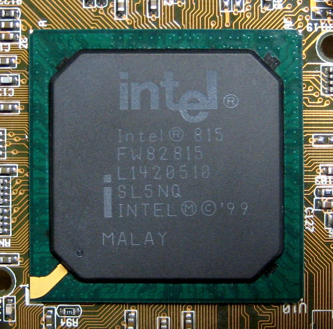 82815 is Intel's north bridge chip.
The
product definition process for that chip illustrates a radical difference between the Intel of
then and the Intel of today. His boss, Joe Friedrich, prepared a single page document
called a Target Specification (spec) that gave the four-digit name to the product. It also
gave the pinout and defined the function in sufficient detail for the approving parties to
decide whether they wanted to build it.
The entire chain of command of Intel, from Robert Noyce on down to Joe Friedrich, met
in a room to decide whether to approve development based on the 5810 Target Spec. In
that single meeting, the decision was made to proceed. The product name, 5810, remained
constant from that point forward throughout the product life. The name appeared in the
Target Spec, the schematics, any memos, the actual layout, the masks, the...