INTEGRATED CIRCUIT TECHNOLOGY
In the early 1970's integrated circuit superseded the construction of electronic circuits assembled by the soldered inter-connected of discrete components such as transistors, diodes, resistors, etc. From this time on most electronic circuits and systems contained some circuitry in the form of monolithic integrated circuit. These so-called 'silicon chips' now form the main operating parts of all electronic systems used in computers, communications, control and instrumentation systems, etc.
The fabrication of integrated circuits were the individual components such as transistors, diodes, resistors, etc. are formed and inter-connected on a single slice of silicon employs several techniques based on photolithography, the controlled diffusion of dopants and a metallic deposition onto the oxidised silicon surface, thereafter, the completed circuit is appropriately packaged to give it environmental immunity.
WAFERS
The whole process starts with the preparation of the silicon wafers. The wafers are thin, circular discs of silicon. They are made in various diameters, 100, 125 and 150mm with even larger ones being developed.
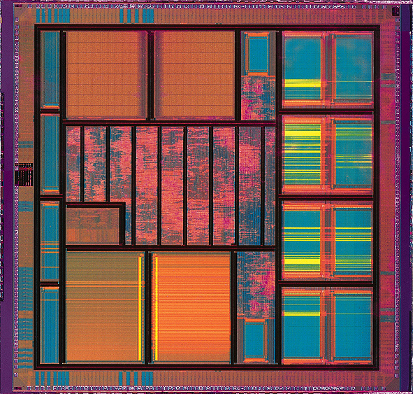 Integrated circuit of Atmel Diopsis 740 System on ...
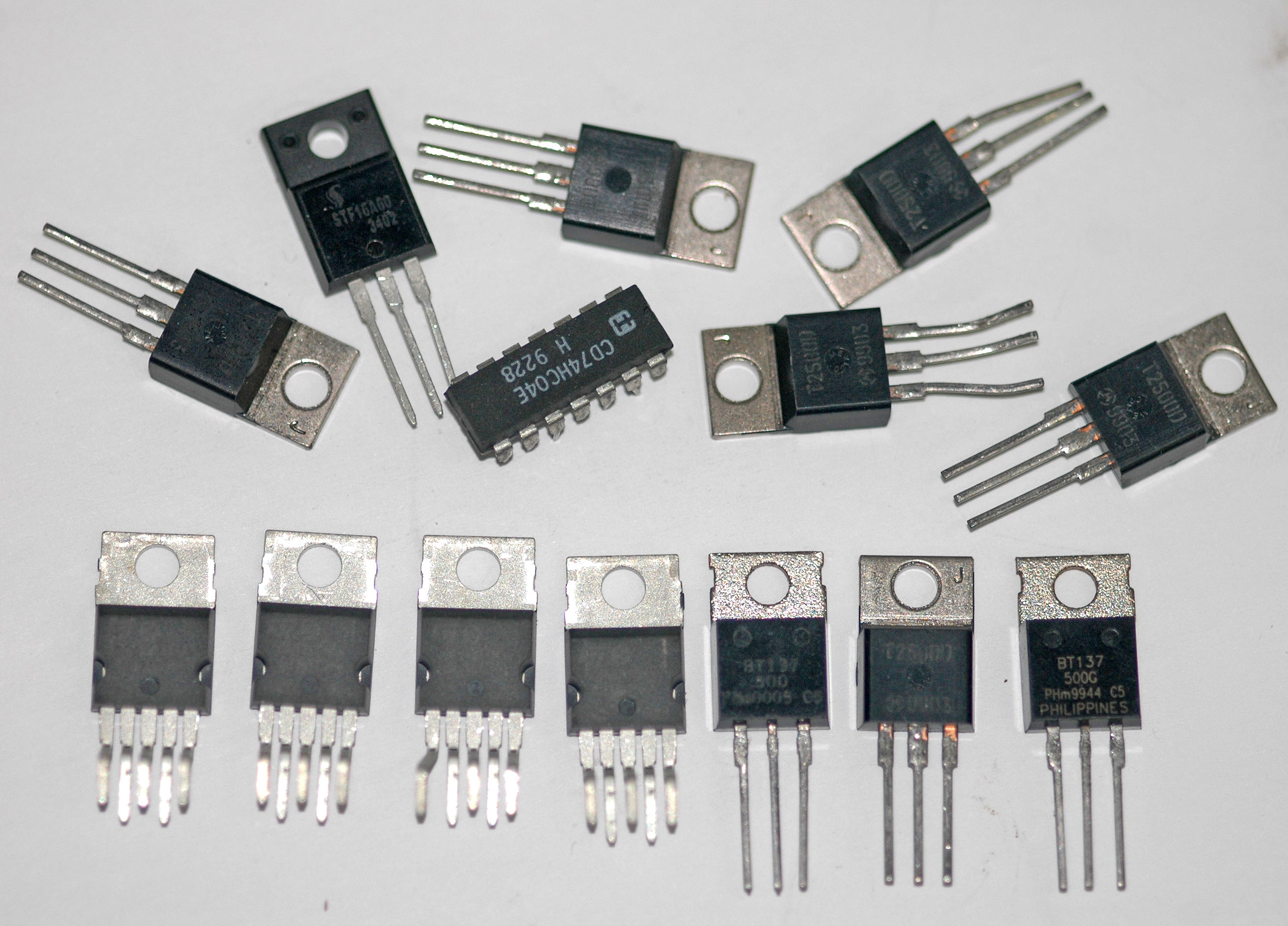 English: Several assorted integrated circuit chips...
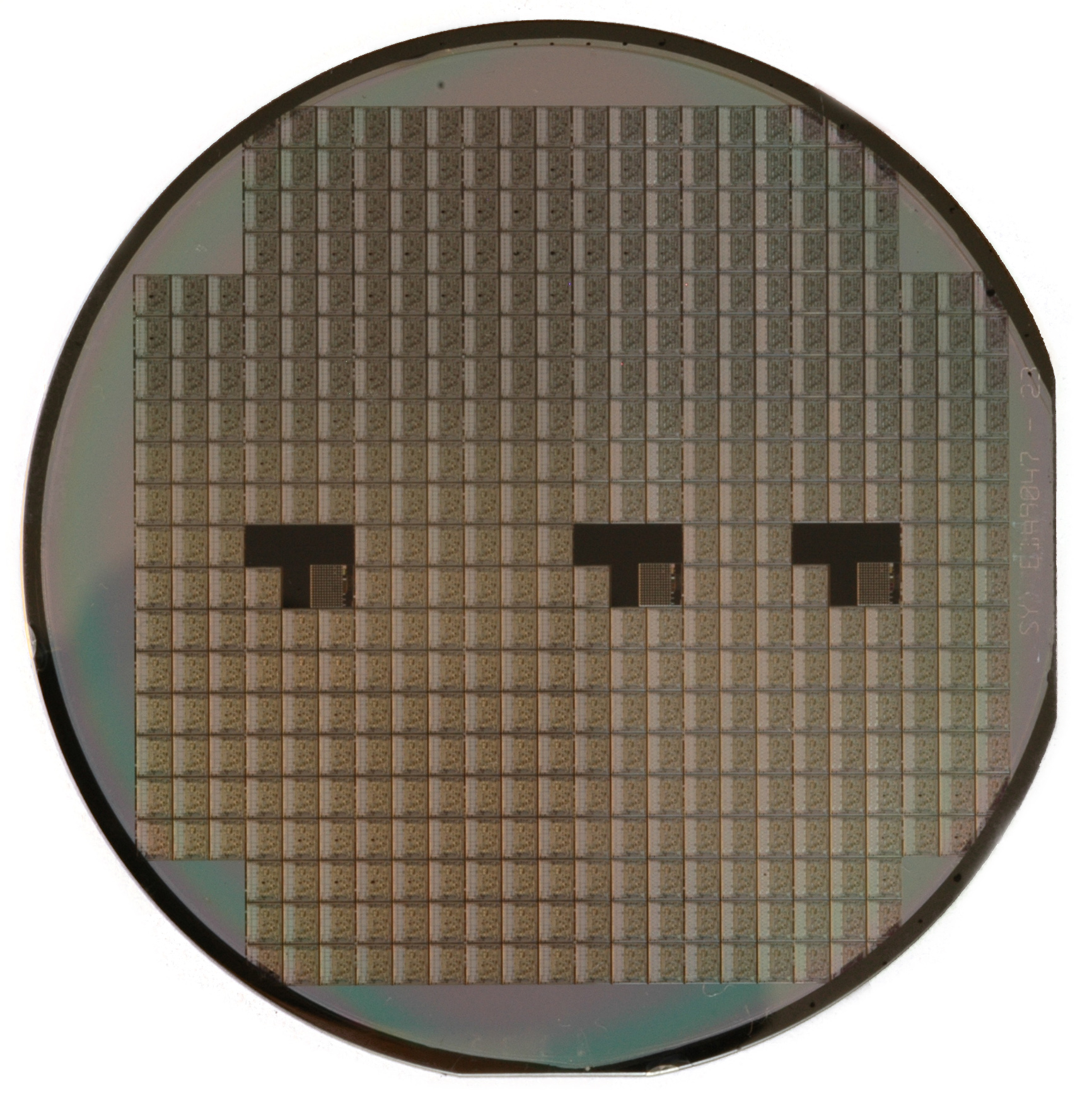 English: Photograph of a silicon wafer.
The wafers are normally less than 1mm in thickness.
The individual wafers are sawn from long cylindrical rods of silicon with the use of laser scribes. The silicon rods may be as much as 3m in length. The silicon rods are made by crystal pulling techniques.
CRYSTAL PULLING
Silicon crystals are grown under very stringent conditions to ensure that they are pure and that the crystal construction is as perfect as possible.
The crystal growth begins with a seed crystal previously cut from another crystal and as the molten silicon at 1400ðC loses heat it solidifies onto the seed crystal. The crystal is then drawn from the melt at a precise rate to form the ingot. Slow growth is essential to maintain a perfect crystalline structure, the growth rate being about 2mm per minute.
As well...